 | ÐлекÑÑоннÑй компоненÑ: OP281 | СкаÑаÑÑ:  PDF PDF  ZIP ZIP |
Äîêóìåíòàöèÿ è îïèñàíèÿ www.docs.chipfind.ru
REV. B
Information furnished by Analog Devices is believed to be accurate and
reliable. However, no responsibility is assumed by Analog Devices for its
use, nor for any infringements of patents or other rights of third parties that
may result from its use. No license is granted by implication or otherwise
under any patent or patent rights of Analog Devices. Trademarks and
registered trademarks are the property of their respective companies.
One Technology Way, P.O. Box 9106, Norwood, MA 02062-9106, U.S.A.
Tel: 781/329-4700
www.analog.com
Fax: 781/326-8703
© 2003 Analog Devices, Inc. All rights reserved.
OP281/OP481
Ultralow Power, Rail-to-Rail Output
Operational Amplifiers
FEATURES
Low Supply Current: 4 A/Amplifier Max
Single-Supply Operation: 2.7 V to 12 V
Wide Input Voltage Range
Rail-to-Rail Output Swing
Low Offset Voltage: 1.5 mV
No Phase Reversal
APPLICATIONS
Comparator
Battery-Powered Instrumentation
Safety Monitoring
Remote Sensors
Low Voltage Strain Gage Amplifiers
GENERAL DESCRIPTION
The OP281 and OP481 are dual and quad ultralow power, single-
supply amplifiers featuring rail-to-rail outputs. Each operates
from supplies as low as 2.0 V and are specified at +3 V and +5 V
single supply as well as
±5 V dual supplies.
Fabricated on Analog Devices' CBCMOS process, the
OP281/OP481 features a precision bipolar input and an output
that swings to within millivolts of the supplies and continues to
sink or source current all the way to the supplies.
Applications for these amplifiers include safety monitoring,
portable equipment, battery and power supply control, and
signal conditioning and interfacing for transducers in very low
power systems.
The output's ability to swing rail-to-rail and not increase supply
current, when the output is driven to a supply voltage, enables
the OP281/OP481 to be used as comparators in very low power
systems. This is enhanced by their fast saturation recovery time.
Propagation delays are 250
ms.
The OP281/OP481 are specified over the extended industrial
temperature range (40
C to +85C). The OP281 dual amplifier
is available in 8-lead SOIC surface-mount and TSSOP packages.
The OP481 quad amplifier is available in narrow 14-lead SOIC
and TSSOP packages.
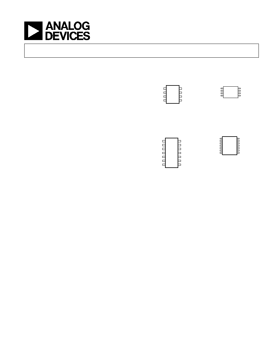
PIN CONFIGURATIONS
14-Lead
Narrow-Body SOIC
(R Suffix)
1
7
8
14
OP481
OUT A
IN A
+IN A
V+
+IN B
IN B
OUT B
OUT D
IN D
+IN D
V
+IN C
IN C
OUT C
8-Lead SOIC
(R Suffix)
OUT A
V+
OUT B
IN A
+IN A
V
+IN B
IN B
1
4
5
8
OP281
14-Lead TSSOP
(RU Suffix)
OP481
1
7
8
14
NOTE: PIN ORIENTATION IS EQUIVALENT FOR
EACH PACKAGE VARIATION
8-Lead TSSOP
(RU Suffix)
OP281
1
4
5
8

REV. B
2
OP281/OP481SPECIFICATIONS
ELECTRICAL SPECIFICATIONS
Parameter
Symbol
Condition
Min
Typ
Max
Unit
INPUT CHARACTERISTICS
Offset Voltage
V
OS
Note 1
1.5
mV
40
C £ T
A
£ +85C
2.5
mV
Input Bias Current
I
B
40
C £ T
A
£ +85C
3
10
nA
Input Offset Current
I
OS
40
C £ T
A
£ +85C
0.1
7
nA
Input Voltage Range
0
2
V
Common-Mode Rejection Ratio
CMRR
V
CM
= 0 V to 2.0 V,
40
C £ T
A
£ +85C
65
95
dB
Large Signal Voltage Gain
A
VO
R
L
= 1 M
W, V
O
= 0.3 V to 2.7 V
5
13
V/mV
40
C £ T
A
£ +85C
2
V/mV
Offset Voltage Drift
V
OS
/DT
10
mV/C
Bias Current Drift
I
B
/DT
20
pA/
C
Offset Current Drift
I
OS
/DT
2
pA/
C
OUTPUT CHARACTERISTICS
Output Voltage High
V
OH
R
L
= 100 k
W to GND,
40
C £ T
A
£ +85C
2.925
2.96
V
Output Voltage Low
V
OL
R
L
= 100 k
W to V+,
40
C £ T
A
£ +85C
25
75
mV
Short Circuit Limit
I
SC
±1.1
mA
POWER SUPPLY
Power Supply Rejection Ratio
PSRR
V
S
= 2.7 V to 12 V,
40
C £ T
A
£ +85C
76
95
dB
Supply Current/Amplifier
I
SY
V
O
= 0 V
3
4
mA
40
C £ T
A
£ +85C
5
mA
DYNAMIC PERFORMANCE
Slew Rate
SR
R
L
= 100 k
W, C
L
= 50 pF
25
V/ms
Turn On Time
A
V
= 1, V
O
= 1
40
ms
Turn On Time
A
V
= 20, V
O
= 1
50
ms
Saturation Recovery Time
65
ms
Gain Bandwidth Product
GBP
95
kHz
Phase Margin
o
70
Degrees
NOISE PERFORMANCE
Voltage Noise
e
n
p-p
0.1 Hz to 10 Hz
10
mV p-p
Voltage Noise Density
e
n
f = 1 kHz
75
nV/
÷Hz
Current Noise Density
i
n
<1
pA/
÷Hz
*V
OS
is tested under a no load condition.
Specifications subject to change without notice.
(@ V
S
= 3.0 V, V
CM
= 1.5 V, T
A
= 25 C, unless otherwise noted.*)

REV. B
OP281/OP481
3
(@ V
S
= 5.0 V, V
CM
= 2.5 V, T
A
= 25 C, unless otherwise noted.*)
ELECTRICAL SPECIFICATIONS
Parameter
Symbol
Condition
Min
Typ
Max
Unit
INPUT CHARACTERISTICS
Offset Voltage
V
OS
Note 1
0.1
1.5
mV
40
°C T
A
+85°C
2.5
mV
Input Bias Current
I
B
40
°C T
A
+85°C
3
10
nA
Input Offset Current
I
OS
40
°C T
A
+85°C
0.1
7
nA
Input Voltage Range
0
4
V
Common-Mode Rejection Ratio
CMRR
V
CM
= 0 V to 4.0 V,
40
°C T
A
+85°C
65
90
dB
Large Signal Voltage Gain
A
VO
R
L
= 1 M
, V
O
= 0.5 V to 4.5 V
5
15
V/mV
40
°C T
A
+85°C
2
V/mV
Offset Voltage Drift
V
OS
/DT
40
°C to +85°C
10
µV/°C
Bias Current Drift
I
B
/DT
20
pA/
°C
Offset Current Drift
I
OS
/DT
2
pA/
°C
OUTPUT CHARACTERISTICS
Output Voltage High
V
OH
R
L
= 100 k
to GND,
40
°C T
A
+85°C
4.925
4.96
V
Output Voltage Low
V
OL
R
L
= 100 k
to V+,
40
°C T
A
+85°C
25
75
mV
Short Circuit Limit
I
SC
±3.5
mA
POWER SUPPLY
Power Supply Rejection Ratio
PSRR
V
S
= 2.7 V to 12 V,
40
°C T
A
+85°C
76
95
dB
Supply Current/Amplifier
I
SY
V
O
= 0 V
3.2
4
µA
40
°C T
A
+85°C
5
µA
DYNAMIC PERFORMANCE
Slew Rate
SR
R
L
= 100 k
, C
L
= 50 pF
27
V/ms
Saturation Recovery Time
120
µs
Gain Bandwidth Product
GBP
100
kHz
Phase Margin
o
74
Degrees
NOISE PERFORMANCE
Voltage Noise
e
n
p-p
0.1 Hz to 10 Hz
10
µV p-p
Voltage Noise Density
e
n
f = 1 kHz
75
nV/
Hz
Current Noise Density
i
n
<1
pA/
Hz
*V
OS
is tested under a no load condition.
Specifications subject to change without notice.

REV. B
4
OP281/OP481
(@ V
S
= 5.0 V, T
A
= +25 C, unless otherwise noted.*)
ELECTRICAL SPECIFICATIONS
Parameter
Symbol
Condition
Min
Typ
Max
Unit
INPUT CHARACTERISTICS
Offset Voltage
V
OS
Note 1
0.1
1.5
mV
40
C £ T
A
£ +85C
2.5
mV
Input Bias Current
I
B
40
C £ T
A
£ +85C
3
10
nA
Input Offset Current
I
OS
40
C £ T
A
£ +85C
0.1
7
nA
Input Voltage Range
5
+4
V
Common-Mode Rejection
CMRR
V
CM
= 5.0 V to +4.0 V,
40
C £ T
A
£ +85C
65
95
dB
Large Signal Voltage Gain
A
VO
R
L
= 1 M
W, V
O
=
±4.0 V,
5
13
V/mV
40
C £ T
A
£ +85C
2
V/mV
Offset Voltage Drift
V
OS
/DT
40
C to +85C
10
mV/C
Bias Current Drift
I
B
/DT
20
pA/
C
Offset Current Drift
I
OS
/DT
2
pA/
C
OUTPUT CHARACTERISTICS
Output Voltage Swing
V
O
R
L
= 100 k
W to GND,
40
C £ T
A
£ +85C
±4.925
±4.98
V
Short Circuit Limit
I
SC
12
mA
POWER SUPPLY
Power Supply Rejection Ratio
PSRR
V
S
=
±1.35 V to ±6 V,
40
C £ T
A
£ +85C
76
95
dB
Supply Current/Amplifier
I
SY
V
O
= 0 V
3.3
5
mA
40
C £ T
A
£ +85C
6
mA
DYNAMIC PERFORMANCE
Slew Rate
±SR
R
L
= 100 k
W, C
L
= 50 pF
28
V/ms
Gain Bandwidth Product
GBP
105
kHz
Phase Margin
o
75
Degrees
NOISE PERFORMANCE
Voltage Noise
e
n
p-p
0.1 Hz to 10 Hz
10
mV p-p
Voltage Noise Density
e
n
f = 1 kHz
85
nV/
÷Hz
Voltage Noise Density
e
n
f = 10 kHz
75
nV/
÷Hz
Current Noise Density
i
n
<1
pA/
÷Hz
*V
OS
is tested under a no load condition.
Specifications subject to change without notice.

REV. B
OP281/OP481
5
ORDERING GUIDE
Temperature
Package
Package
Model
Range
Description
Option
OP281GS
40
C to +85C 8-Lead SOIC
R-8
OP281GRU
40
C to +85C 8-Lead TSSOP
RU-8
OP481GS
40
C to +85C 14-Lead SOIC
R-14
OP481GRU
40
C to +85C 14-Lead TSSOP RU-14
ABSOLUTE MAXIMUM RATINGS
*
Supply Voltage . . . . . . . . . . . . . . . . . . . . . . . . . . . . . . . . . 16 V
Input Voltage . . . . . . . . . . . . . . . . . . . . . . . GND to V
S
+ 10 V
Differential Input Voltage . . . . . . . . . . . . . . . . . . . . . .
±3.5 V
Output Short-Circuit Duration to GND . . . . . . . . . Indefinite
Storage Temperature Range . . . . . . . . . . . . 65
C to +150C
Operating Temperature Range . . . . . . . . . . . 40
C to +85C
Junction Temperature Range . . . . . . . . . . . . 65
C to +150C
Lead Temperature Range (Soldering, 60 sec) . . . . . . . . 300
C
*Stresses above those listed under Absolute Maximum Ratings may cause perma-
nent damage to the device. This is a stress rating only; functional operation of the
device at these or any other conditions above those listed in the operational
sections of this specification is not implied. Exposures to absolute maximum rating
conditions for extended periods may affect device reliability.
Package Type
JA
*
JC
Unit
8-Lead SOIC (R)(S)
158
43
C/W
8-Lead TSSOP (RU)
240
43
C/W
14-Lead SOIC (R)(S)
120
3 6
C/W
14-Lead TSSOP (RU)
240
43
C/W
*
q
JA
is specified for the worst-case conditions, i.e.,
q
JA
is specified for device
soldered in circuit board for TSSOP and SOIC packages.
CAUTION
ESD (electrostatic discharge) sensitive device. Electrostatic charges as high as 4000 V readily
accumulate on the human body and test equipment and can discharge without detection. Although the
OP281/OP481 features proprietary ESD protection circuitry, permanent damage may occur on
devices subjected to high energy electrostatic discharges. Therefore, proper ESD precautions are
recommended to avoid performance degradation or loss of functionality.
REV. B
6
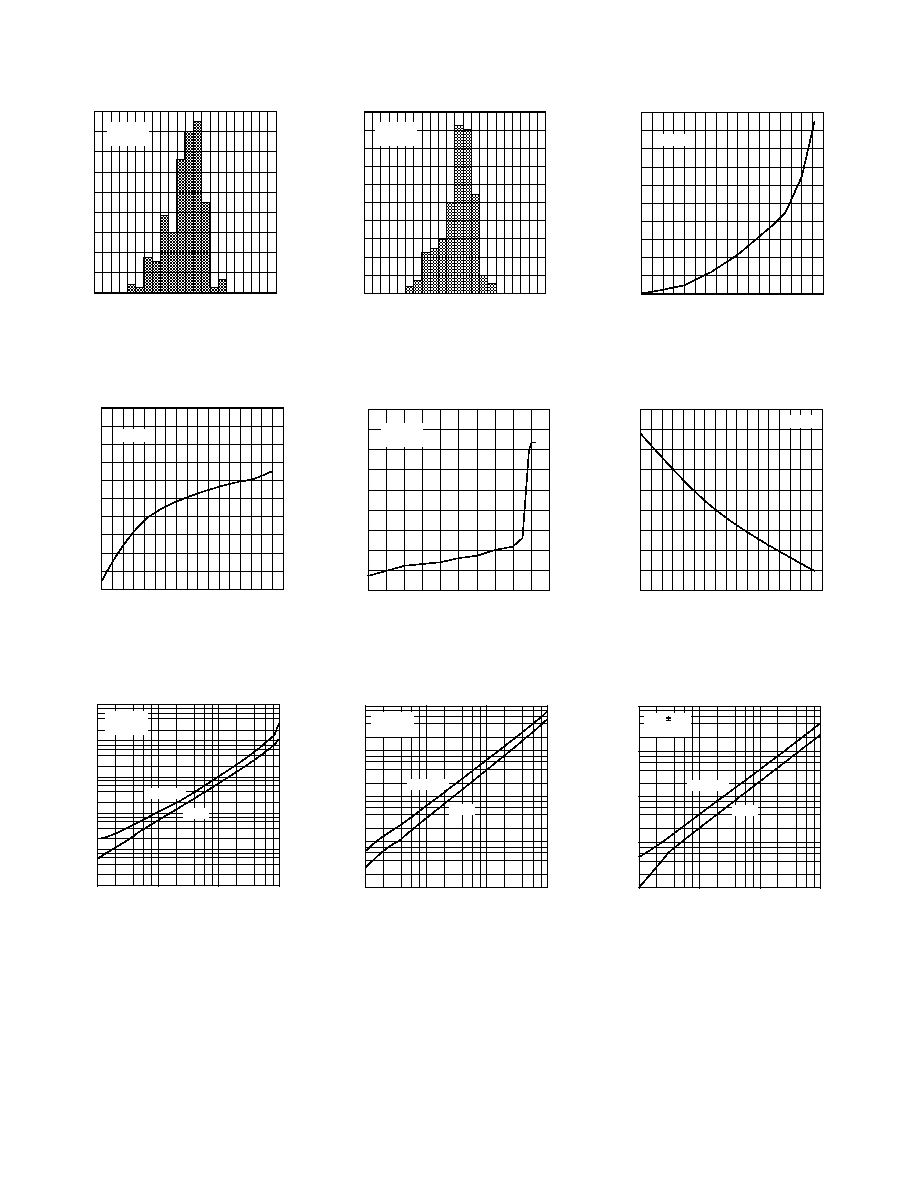
OP281/OP481Typical Performance Characteristics
1.0 0.8 0.60.4 0.2
0
0.2 0.4 0.6 0.8 1.0
INPUT OFFSET VOLTAGE mV
QUANTITY Amplifiers
45
40
0
20
15
10
5
35
25
30
V
S
= 2.7V
T
A
= 25 C
TPC 1. Input Offset Voltage
Distribution
TEMPERATURE C
0
3.5
5.0
40 20
0
20
40
60
80
0.5
3.0
4.0
4.5
1.0
2.0
1.5
2.5
100 120
INPUT BIAS CURRENT nA
V
S
= 5V
TPC 4. Input Bias Current
vs. Temperature
LOAD CURRENT µA
OUTPUT VOLTAGE mV
10,000
1,000
0.1
1
1000
10
100
100
10
1.0
SOURCE
SINK
V
S
= 3V
T
A
= 25 C
TPC 7. Output Voltage to
Supply Rail vs. Load Current
INPUT OFFSET VOLTAGE mV
1.0 0.8 0.60.4 0.2
0
0.2 0.4 0.6 0.8 1.0
QUANTITY Amplifiers
45
40
0
20
15
10
5
35
25
30
V
S
= 5V
T
A
= 25 C
50
TPC 2. Input Offset Voltage
Distribution
COMMON-MODE VOLTAGE V
INPUT BIAS CURRENT nA
1.0
2.0
3.5
0.0 0.5 1.0 1.5 2.0 2.5 3.0
1.5
2.5
3.0
0.5
0.5
0.0
1.0
3.5 4.0
V
S
= 5V
T
A
= 25 C
4.5 5.0
TPC 5. Input Bias Current
vs. Common-Mode Voltage
LOAD CURRENT µA
OUTPUT VOLTAGE mV
1,000
0.1
1
1000
10
100
100
10
1.0
SOURCE
SINK
V
S
= 5V
T
A
= 25 C
TPC 8. Output Voltage to
Supply Rail vs. Load Current
TEMPERATURE C
INPUT OFFSET VOLTAGE µ
V
2000
600
0
40 20
0
20
40
60
80
1800
800
400
200
1600
1200
1400
1000
100 120
V
S
= 5V
TPC 3. Input Offset Voltage
vs. Temperature
TEMPERATURE C
INPUT OFFSET CURRENT nA
0.5
0.1
0.4
40 20
0
20
40
60
80
0
0.2
0.3
0.4
0.2
0.3
0.1
100 120
V
S
= 5V
TPC 6. Input Offset Current
vs. Temperature
LOAD CURRENT µA
OUTPUT VOLTAGE mV
1,000
0.1
1
1000
10
100
100
10
1.0
SOURCE
SINK
V
S
= 5V
T
A
= +25 C
TPC 9. Output Voltage to
Supply Rail vs. Load Current
REV. B
OP281/OP481
7
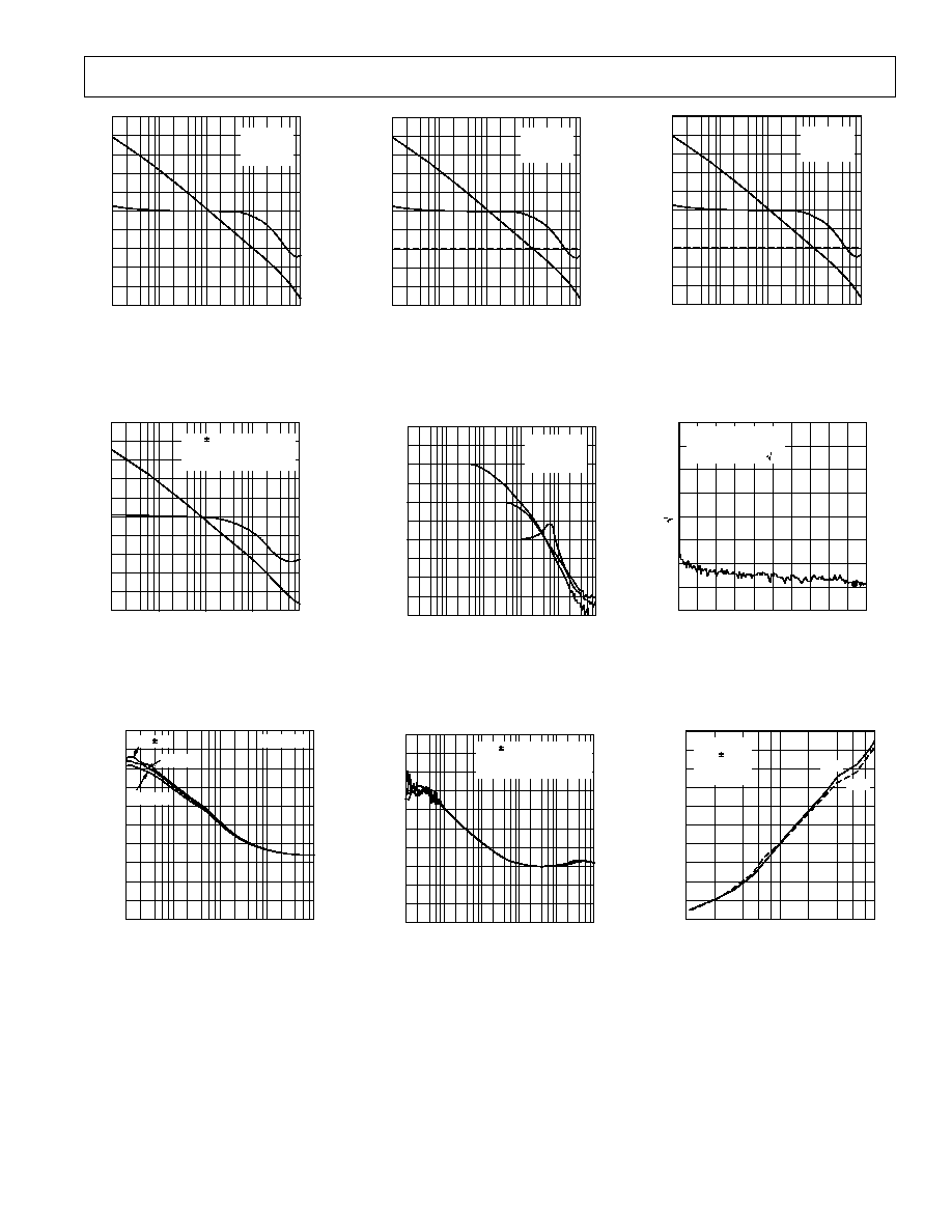
FREQUENCY Hz
OPEN-LOOP GAIN dB
70
60
30
100
1k
1M
10k
100k
20
50
40
30
10
0
10
20
V
S
= 5V
T
A
= 25 C
R
L
= 100k
90
0
45
135
180
225
270
PHASE SHIFT Degrees
TPC 10. Open-Loop Gain
and Phase vs. Frequency
FREQUENCY Hz
OPEN-LOOP GAIN dB
70
60
30
100
1k
1M
10k
100k
20
50
40
30
10
0
10
20
V
S
= 5V
T
A
= +25 C
R
L
= 100k TO GROUND
90
0
45
135
180
225
270
PHASE SHIFT Degrees
TPC 13. Open-Loop Gain
and Phase vs. Frequency
FREQUENCY Hz
CMRR dB
1k
10k
10M
100k
1M
90
80
10
70
60
50
40
30
20
10
0
T
A
= +25 C
V
S
= 5V
V
S
= +5V
V
S
= +3V
TPC 16. CMRR vs. Frequency
FREQUENCY Hz
OPEN-LOOP GAIN dB
70
60
30
100
1k
1M
10k
100k
20
50
40
30
10
0
10
20
V
S
= 2.7V
T
A
= 25 C
R
L
= 100k
90
0
45
135
180
225
270
PHASE SHIFT Degrees
TPC 12. Open-Loop Gain
and Phase vs. Frequency
FREQUENCY Hz
V
S
= 5V
T
A
= 25 C
MARKER @ 67nV/ Hz
0
2k
4k
6k
8k
10k
50nV/
Hz/
Div
TPC 15. Voltage Noise Density
vs. Frequency
CAPACITANCE pF
SMALL SIGNAL OVERSHOOT %
50
45
0
10
100
1000
40
35
30
25
20
15
10
5
V
S
= +5V
V
IN
= 50mV
R
L
= 100k
T
A
= +25 C
OS
+OS
TPC 18. Small Signal Overshoot
vs. Load Capacitance
FREQUENCY Hz
OPEN-LOOP GAIN dB
70
60
30
100
1k
1M
10k
100k
20
50
40
30
10
0
10
20
V
S
= 3V
T
A
= 25 C
R
L
= 100k
90
0
45
135
180
225
270
PHASE SHIFT Degrees
TPC 11. Open-Loop Gain
and Phase vs. Frequency
FREQUENCY Hz
CLOSED-LOOP GAIN dB
10
100
1M
1k
10k
100k
60
50
40
40
30
20
10
0
10
20
30
V
S
= 5V
T
A
= 25 C
R
L
= INFINITE
TPC 14. Closed-Loop Gain vs.
Frequency
FREQUENCY Hz
PSRR dB
10
100
1M
1k
10k
100k
160
140
40
120
100
80
60
40
20
0
20
V
S
= 5V, +5V, +3V, +2.7V
T
A
= +25 C
R
L
= INFINITE
TPC 17. PSRR vs. Frequency
REV. B
8
OP281/OP481
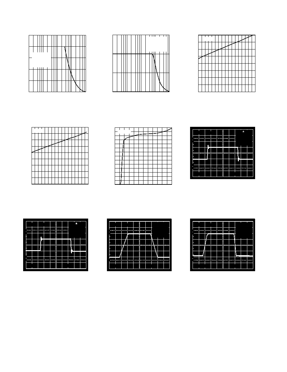
FREQUENCY Hz
5
4
0
10
100
100k
1k
10k
3
2
1
MAXIMUM OUTPUT SWING V p-p
V
S
= 5V
V
IN
= 4V p-p
R
L
= INFINITE
T
A
= 25 C
TPC 19. Maximum Output
Swing vs. Frequency
TEMPERATURE C
SUPPLY CURRENT/AMPLIFIER
A
4.5
1.5
0
40 20
0
20
40
60
80
100 120
3.5
2.0
1.0
0.5
3.0
2.5
V
S
= 5V
4.0
TPC 22. Supply Current/Amplifier
vs. Temperature
10
0%
100
90
0mV
A2
100µs
50mV
V
S
= 1.35V
A
V
= 1
R
L
= 100k
C
L
= 50pF
T
A
= +25 C
TPC 25. Small Signal Transient
Response
TEMPERATURE C
SUPPLY CURRENT/AMPLIFIER
A
4.0
1.5
0
40 20
0
20
40
60
80
100 120
3.5
2.0
1.0
0.5
3.0
2.5
V
S
= 3V
TPC 21. Supply Current/Amplifier
vs. Temperature
10
0%
100
90
0mV
A2
100µs
50mV
V
S
= 2.5V
A
V
= 1
R
L
= 100k
C
L
= 50pF
T
A
= +25 C
TPC 24. Small Signal Transient
Response
10
0%
100
90
0.50V
A2
100µs
500mV
V
S
= 2.75V
A
V
= 1
R
L
= 100k
C
L
= 50pF
T
A
= 25 C
TPC 27. Large Signal Transient
Response
FREQUENCY Hz
3
0
10
100
100k
1k
10k
2
1
MAXIMUM OUTPUT SWING V p-p
V
S
= 3V
V
IN
= 2V p-p
R
L
= INFINITE
T
A
= 25 C
TPC 20. Maximum Output
Swing vs. Frequency
SUPPLY VOLTAGE V
SUPPLY CURRENT/AMPLIFIER
A
3.50
2.00
0.00
0.0 0.5 1.0 1.5 2.0 2.5 3.0 3.5 4.0
3.00
2.25
1.75
1.50
2.75
2.50
T
A
= 25 C
3.25
0.75
1.00
0.50
0.25
1.25
4.5 5.0 5.5 6.0
TPC 23. Supply Current/Amplifier
vs. Supply Voltage
10
0%
100
90
2.50V
A2
100µs
1V
V
S
= 5V
A
V
= 1
R
L
= 100k
C
L
= 50pF
T
A
= 25 C
TPC 26. Large Signal Transient
Response
REV. B
OP281/OP481
9
10
0%
100
90
2.50V
A2
200µs
1V
1V
V
S
= 5V
T
A
= 25 C
TPC 28. No Phase Reversal
10
0%
100
90
0.00V
A2
50µs
500mV
500mV
V
S
= 1.35V
R
L
=
V
IN
= 1V p-p
AT = 2kHz
TPC 29. Saturation Recovery Time
FREQUENCY Hz
CHANNEL SEPARATION dB
100
1k
1M
10k
100k
120
105
30
90
75
60
45
30
15
0
15
V
S =
5V
T
A =
25 C
R
L =
·
TPC 31. Channel Separation
vs. Frequency
100
90
0.00V
A2
100µs
1V
500mV
V
S
= 2.5V
T
A
= +25 C
R
L
=
CIRCUIT = A
VOL
10
0%
TPC 30. Saturation Recovery Time
REV. B
10
OP281/OP481
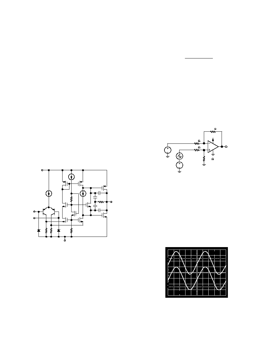
APPLICATIONS
Theory of Operation
The OPx81 family of op amps is comprised of extremely low
powered, rail-to-rail output amplifiers, requiring less than 4
mA
of quiescent current per amplifier. Many other competitors'
devices may be advertised as low supply current amplifiers but
draw significantly more current as the outputs of these devices
are driven to a supply rail. The OPx81's supply current remains
under 4
mA even with the output driven to either supply rail.
Supply currents should meet the specification as long as the
inputs and outputs remain within the range of the power supplies.
Figure 1 shows a simplified schematic of a single channel for the
OPx81. A bipolar differential pair is used in the input stage.
PNP transistors are used to allow the input stage to remain
linear with the common-mode range extending to ground. This
is an important consideration for single-supply applications. The
bipolar front end also contributes less noise than a MOS front
end with only nano-amps of bias currents. The output of the op
amp consists of a pair of CMOS transistors in a common source
configuration. This setup allows the output of the amplifier to
swing to within millivolts of either supply rail. The headroom
required by the output stage is limited by the amount of current
being driven into the load. The lower the output current, the
closer the output can go to either supply rail. TPCs 7, 8, and 9
show the output voltage headroom versus load current. This
behavior is typical of rail-to-rail output amplifiers.
+IN
IN
V
EE
OUT
V
CC
Figure 1. Simplified Schematic of a Single OPx81 Channel
Input Overvoltage Protection
The input stage to the OPx81 family of op amps consists of a
PNP differential pair. If the base voltage of either of these input
transistors drops to more than 0.6 V below the negative supply,
the input ESD protection diodes will become forward biased,
and large currents will begin to flow. In addition to possibly
damaging the device, this will create a phase reversal effect at
the output. To prevent these effects from happening, the input
current should be limited to less than 0.5 mA.
This can be done quite easily by placing a resistor in series with
the input to the device. The size of the resistor should be pro-
portional to the lowest possible input signal excursion and can
be found using the following formula:
R
=
V
EE
-V
IN , MIN
0.5
¥10
-3
where:
V
EE
is the negative power supply for the amplifier.
V
IN, MIN
is the lowest input voltage excursion expected.
For example, a single channel of the OPx81 is to be used with a
single-supply voltage of +5 V where the input signal could possibly
go as low as 1 V. Because the amplifier is powered from a single
supply, V
EE
is ground, so the necessary series resistance should
be 2 k
W.
Input Offset Voltage
The OPx81 family of op amps was designed for low offset
voltages less than 1 mV.
OP281
V
OUT
+3V
100k
100k
100k
100k
V
IN
= 1kHz AT
400mV p-p
0.1V
0.27V
Figure 2. Single OPx81 Channel Configured as
a Difference Amplifier Operating at V
CM
< 0 V
Input Common-Mode Voltage Range
The OPx81 is rated with an input common-mode voltage range
from V
EE
to 1 V under V
CC
. However, the op amp can still oper-
ate even with a common-mode voltage that is slightly less than V
EE
.
Figure 2 shows a single OPx81 channel configured as a difference
amplifier with a single-supply voltage of 3 V. Negative dc voltages
are applied at both input terminals creating a common-mode volt-
age that is less than ground. A 400 mV p-p input signal is then
applied to the noninverting input. Figure 3 shows the input and
output waves. Notice how the output of the amplifier also drops
slightly negative without distortion.
10
0%
100
90
0.2ms
0.1V
0V
V
IN
V
OUT
Figure 3. Input and Output Signals with V
CM
< 0 V
REV. B
OP281/OP481
11
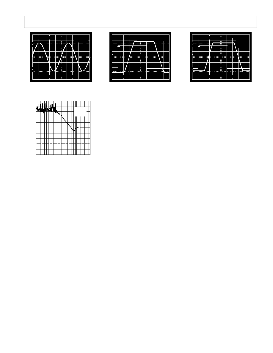
Capacitive Loading
Most low supply current amplifiers have difficulty driving
capacitive loads due to the higher currents required from the
output stage for such loads. Higher capacitance at the output
will increase the amount of overshoot and ringing in the amplifier's
step response and could even affect the stability of the device.
However, through careful design of the output stage and its
high phase margin, the OPx81 family can tolerate some degree of
capacitive loading. Figure 4 shows the step response of a single
channel with a 10 nF capacitor connected at the output. Notice
that the overshoot of the output does not exceed more than 10%
with such a load, even with a supply voltage of only 3 V.
10
0%
100
90
Figure 4. Ringing and Overshoot of the Output
of the Amplifier
Micropower Reference Voltage Generator
Many single-supply circuits are configured with the circuit biased
to 1/2 of the supply voltage. In these cases, a false ground refer-
ence can be created by using a voltage divider buffered by an
amplifier. Figure 5 shows the schematic for such a circuit.
The two 1 M
W resistors generate the reference voltage while
drawing only 1.5
mA of current from a 3 V supply. A capacitor
connected from the inverting terminal to the output of the op amp
provides compensation to allow for a bypass capacitor to be
connected at the reference output. This bypass capacitor helps
to establish an ac ground for the reference output. The entire
reference generator draws less than 5
mA from a 3 V supply source.
1
8
4
2
3
OP281
10k
0.022 F
V
REF
1.5V TO 6V
1 F
1 F
1M
3V TO 12V
100
1M
Figure 5. Single Channel Configured as a Micropower
Bias Voltage Generator
Window Comparator
The extremely low power supply current demands of the OPx81
family make it ideal for use in long-life battery-powered applica-
tions such as a monitoring system. Figure 6 shows a circuit that
uses the OP281 as a window comparator.
A1
R1
R2
3V
OP281-A
V
IN
2k
5.1k
3V
3V
V
OUT
Q1
5.1k
V
H
D1
10k
A2
R3
R4
3V
3V
V
L
D2
OP281-B
Figure 6. Using the OP281 as a Window Comparator
The threshold limits for the window are set by V
H
and V
L
, pro-
vided that V
H
> V
L
. The output of A1 will stay at the negative
rail, in this case ground, as long as the input voltage is less than
V
H
. Similarly, the output of A2 will stay at ground as long the
input voltage is higher than V
L
. As long as V
IN
remains between
V
L
and V
H
, the outputs of both op amps will be 0 V. With no
current flowing in either D1 or D2, the base of Q1 will stay at
ground, putting the transistor in cutoff and forcing V
OUT
to the
positive supply rail. If the input voltage rises above V
H
, the
output of A2 stays at ground, but the output of A1 will go to the
positive rail, and D1 will conduct current. This creates a base
voltage that will turn on Q1 and drive V
OUT
low. The same
condition occurs if V
IN
falls below V
L
with A2's output going
high, and D2 conducting current. Therefore, V
OUT
will be high
if the input voltage is between V
L
and V
H
, and V
OUT
will be low
if the input voltage moves outside of that range.
The R1 and R2 voltage divider sets the upper window voltage,
and the R3 and R4 voltage divider sets the lower voltage for the
window. For the window comparator to function properly, V
H
must be a greater voltage than V
L
.
V
H
=
R2
R1
+ R2
V
L
=
R4
R3
+ R4
The 2 k
W resistor connects the input voltage to the input terminals
to the op amps. This protects the OP281 from possible excess
current flowing into the input stages of the devices. D1 and D2 are
small-signal switching diodes (1N4446 or equivalent), and Q1
is a 2N2222 or equivalent NPN transistor.
REV. B
12
OP281/OP481
Low-Side Current Monitor
In the design of power supply control circuits, a great deal of
design effort is focused on ensuring a pass transistor's long-term
reliability over a wide range of load current conditions. As a
result, monitoring and limiting device power dissipation is of
prime importance in these designs. Figure 7 shows an example
of a 5 V, single-supply current monitor that can be incorporated
into the design of a voltage regulator with fold-back current
limiting or a high current power supply with crowbar protection.
The design capitalizes on the OPx81's common-mode range
that extends to ground. Current is monitored in the power sup-
ply return path where a 0.1
W shunt resistor, R
SENSE
, creates a
very small voltage drop. The voltage at the inverting terminal
becomes equal to the voltage at the noninverting terminal through
the feedback of Q1, which is a 2N2222 or equivalent NPN tran-
sistor. This makes the voltage drop across R1 equal to the voltage
drop across R
SENSE
. Therefore, the current through Q1 becomes
directly proportional to the current through R
SENSE
, and the output
voltage is given by:
V
OUT
= V
EE
-
R2
R1 ¥
R
SENSE
¥ I
L
Ê
Ë
Á
^
¯
~
The voltage drop across R2 increases with I
L
increasing, so V
OUT
decreases with higher supply current being sensed. For the
element values shown, the V
OUT
transfer characteristic is 2.5 V/A,
decreasing from V
EE
.
5V
RETURN TO
GROUND
5V
R2
2.49k
V
OUT
R1
100
0.1
R
SENSE
Q1
SINGLE
CHANNEL
OPx81
Figure 7. Low-Side Load Current Monitor
Low Voltage Half-Wave and Full-Wave Rectifiers
Because of its quick overdrive recovery time, an OP281 can be
configured as a full-wave rectifier for low frequency (<500 Hz)
applications. Figure 8 shows the schematic.
3V
OP281-A
V
IN
= 2V p-p
2k
A1
3V
OP281-B
A2
R1 = 100k
R2 = 100k
FULL-WAVE
RECTIFIED
OUTPUT
HALF-WAVE
RECTIFIED
OUTPUT
Figure 8. Single-Supply Full-Wave and Half-Wave
Rectifiers Using an OP281
10
0%
100
90
SCALE 0.1V/DIV
SCALE 0.1ms/DIV
Figure 9. Full-Wave Rectified Signal
Amplifier A1 is used as a voltage follower that will track the input
voltage only when it is greater than 0 V. This provides a half-wave
rectification of the input signal to the noninverting terminal of
amplifier A2. When A1's output is following the input, the invert-
ing terminal of A2 will also follow the input from the virtual
ground between the inverting and noninverting terminals of A2.
With no potential difference across R1, no current flows through
either R1 or R2, therefore the output of A2 will also follow the input.
Now, when the input voltage goes below 0 V, the noninverting
terminal of A2 becomes 0 V. This makes A2 work as an inverting
amplifier with a gain of 1 and provides a full-wave rectified version
of the input signal. A 2 k
W resistor in series with A1's noninverting
input protects the device when the input signal becomes less
than ground.
Battery-Powered Telephone Headset Amplifier
Figure 10 shows how the OP281 can be used as a two-way
amplifier in a telephone headset. One side of the OP281 can be
used as an amplifier for the microphone, while the other side can
be used to drive the speaker. A typical telephone headset uses a
600
W speaker and an electret microphone that requires a supply
voltage and a biasing resistor.
3V
OP281-B
20k
20k
Q1
Q2
3V
1 F
600
SPEAKER
50k
10k
1 F
10k
POT.
3V
1M
1M
1 F
1 F
INPUT
1M
3V
OP281-A
11k
300k
0.1 F
1 F
3V
1M
1 F
MIC OUT
2.2k
3V
ELECTRET
MIC
Figure 10. Two-Way Amplifier in a Battery-Powered
Telephone Headset

REV. B
OP281/OP481
13
The OP281-A op amp provides about 29 dB of gain for audio
signals coming from the microphone. The gain is set by the
300 k
W and 11 kW resistors. The gain bandwidth product of the
amplifier is 95 kHz, which, for the set gain of 28, yields a 3 dB
rolloff at 3.4 kHz. This is acceptable since telephone audio is band
limited for 300 kHz to 3 kHz signals. If higher gain is required
for the microphone, an additional gain stage should be used, as
adding any more gain to the OP281 would limit the audio band-
width. A 2.2 k
W resistor is used to bias the electret microphone.
This resistor value may vary depending on the specifications on
the microphone being used. The output of the microphone is ac-
coupled to the noninverting terminal of the op amp. Two 1 M
W
resistors are used to provide the dc offset for single-supply use.
The OP281-B amplifier can provide up to 15 dB of gain for the
headset speaker. Incoming audio signals are ac-coupled to a
10 k
W potentiometer that is used to adjust the volume. Again,
two 1 M
W resistors provide the dc offset with a 1 mF capacitor
establishing an ac ground for the volume control potentiometer.
Because the OP281 is a rail-to-rail output amplifier, it would have
difficulty driving a 600
W speaker directly. Here, a class AB buffer
is used to isolate the load from the amplifier and also provide
the necessary current drive to the speaker. By placing the buffer
in the feedback loop of the op amp, crossover distortion can be
minimized. Q1 and Q2 should have minimum betas of 100. The
600
W speaker is ac-coupled to the emitters to prevent any qui-
escent current from flowing in the speaker. The 1
mF coupling
capacitor makes an equivalent high-pass filter cutoff at 265 Hz
with a 600
W load attached. Again, this does not pose a problem,
as it is outside the frequency range for telephone audio signals.
The circuit in Figure 10 draws around 250
mA of current. The
class AB buffer has a quiescent current of 140
mA while roughly
100
mA is drawn by the microphone itself. A CR2032 3 V lithium
battery has a life expectancy of 160 mA hours, which means this
circuit could run continuously for 640 hours on a single battery.
SPICE Macro-Model
Single OPx81 Channel SPICE Macro-model
* 9/96, Ver. 1
*
* Copyright 1996 by Analog Devices
*
* Refer to "README.DOC" file for License Statement. Use of this
* model indicates your acceptance of the terms and provisions in the
* License Statement.
*
* Node Assignments
*
noninverting input
*
|
inverting input
*
|
|
positive supply
*
|
|
|
negative supply
*
|
|
|
|
output
*
|
|
|
|
|
*
|
|
|
|
|
.SUBCKT OPx81
1
2
99
50
45
*
* INPUT STAGE
*
Q1
4
1
3
PIX
Q2
6
7
5
PIX
I1
99
8
1.28E-6
EOS
7
2
POLY(1)
(12, 98) 80E-6 1
IOS
1
2
1E-10
RC1
4
50
500E3
RC2
6
50
500E3
RE1
3
8
108
RE2
5
8
108
V1
99
13
DC .9
V2
99
14
DC .9
D1
3
13
DX
D2
5
14
DX
*
* CMRR 76dB,
ZERO AT 1kHz
*
ECM1 11 98
POLY(2)
(1, 98) (2, 98) 0 .5 .5
R1
11 12
1.59E6
C1
11 12
100E-12
R2
12 98
283
*
* POLE AT 900kHz
*
EREF 98
0
(90, 0)
1
G1
98 20
(4, 6)
1E-6
R3
20 98
1E6
C2
20 98
177E-15
*
* POLE AT 500kHz
*
E2
21 98
(20, 98)
1
R4
21 22
1E6
C3
22 98
320E-15
*
* GAIN STAGE
*
CF
45
40
8. 5E-12
R5
40
98
65. 65E6
G3
98
40
(22, 98)
4.08E-7
D3
40
41
DX
D4
42
40
DX
V3
99
41
DC 0.5
V4
42
50
DC 0.5
*
* OUTPUT STAGE
*
ISY
99
50
1.375E-6
RS1
99
90
10E6
RS2
90
50
10E6
M1
45
46
99
99
POX L=1.5u
W=300u
M2
45
47
50
50
NOX L=1.5u
W=300u
EG1
99
46
POLY(1)
(98, 40)
0.77
1
EG2
47
50
POLY(1)
(40, 98)
0.77
1
*
* MODELS
*
.MODEL POX PMOS (LEVEL=2, KP=25E-6, VTO=-0.75,
LAMBDA=0.01)
.MODEL NOX NMOS (LEVEL=2, KP=25E-6, VTO=0.75,
LAMBDA=0.01)
.MODEL PIX
PNP
(BF=200)
.MODEL DX D(IS=1E-14)
.ENDS
REV. B
14
OP281/OP481
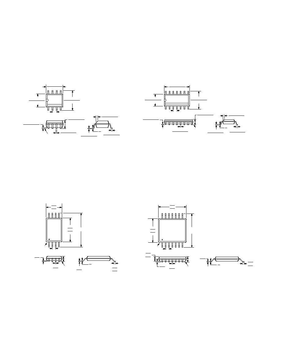
14-Lead Standard Small Outline Package [SOIC]
Narrow Body
(R-14)
Dimensions shown in millimeters and (inches)
CONTROLLING DIMENSIONS ARE IN MILLIMETERS; INCH DIMENSIONS
(IN PARENTHESES) ARE ROUNDED-OFF MILLIMETER EQUIVALENTS FOR
REFERENCE ONLY AND ARE NOT APPROPRIATE FOR USE IN DESIGN
COPLANARITY
0.10
14
8
7
1
6.20 (0.2441)
5.80 (0.2283)
4.00 (0.1575)
3.80 (0.1496)
8.75 (0.3445)
8.55 (0.3366)
1.27 (0.0500)
BSC
SEATING
PLANE
0.25 (0.0098)
0.10 (0.0039)
0.51 (0.0201)
0.33 (0.0130)
1.75 (0.0689)
1.35 (0.0531)
8
0
0.50 (0.0197)
0.25 (0.0098)
45
1.27 (0.0500)
0.40 (0.0157)
0.25 (0.0098)
0.19 (0.0075)
COMPLIANT TO JEDEC STANDARDS MS-012AB
14-Lead Thin Shrink Small Outline Package [TSSOP]
(RU-14)
Dimensions shown in millimeters
4.50
4.40
4.30
14
8
7
1
6.40
BSC
PIN 1
5.10
5.00
4.90
0.65
BSC
SEATING
PLANE
0.15
0.05
0.30
0.19
1.20
MAX
1.05
1.00
0.80
0.20
0.09
8
0
0.75
0.60
0.45
COMPLIANT TO JEDEC STANDARDS MO-153AB-1
COPLANARITY
0.10
OUTLINE DIMENSIONS
8-Lead Standard Small Outline Package [SOIC]
Narrow Body
(R-8)
Dimensions shown in millimeters and (inches)
0.25 (0.0098)
0.19 (0.0075)
1.27 (0.0500)
0.41 (0.0160)
0.50 (0.0196)
0.25 (0.0099)
45
8
0
1.75 (0.0688)
1.35 (0.0532)
SEATING
PLANE
0.25 (0.0098)
0.10 (0.0040)
8
5
4
1
5.00 (0.1968)
4.80 (0.1890)
4.00 (0.1574)
3.80 (0.1497)
1.27 (0.0500)
BSC
6.20 (0.2440)
5.80 (0.2284)
0.51 (0.0201)
0.33 (0.0130)
COPLANARITY
0.10
CONTROLLING DIMENSIONS ARE IN MILLIMETERS; INCH DIMENSIONS
(IN PARENTHESES) ARE ROUNDED-OFF MILLIMETER EQUIVALENTS FOR
REFERENCE ONLY AND ARE NOT APPROPRIATE FOR USE IN DESIGN
COMPLIANT TO JEDEC STANDARDS MS-012AA
8-Lead Thin Shrink Small Outline Package [TSSOP]
(RU-8)
Dimensions shown in millimeters
8
5
4
1
PIN 1
0.65
BSC
SEATING
PLANE
0.15
0.05
0.30
0.19
1.20
MAX
0.20
0.09
8
0
6.40 BSC
0.75
0.60
0.45
4.50
4.40
4.30
3.10
3.00
2.90
COPLANARITY
0.10
COMPLIANT TO JEDEC STANDARDS MO-153AA

REV. B
OP281/OP481
15
Revision History
Location
Page
3/03--Data Sheet changed from REV. A to REV. B.
Changes to FEATURES . . . . . . . . . . . . . . . . . . . . . . . . . . . . . . . . . . . . . . . . . . . . . . . . . . . . . . . . . . . . . . . . . . . . . . . . . . . . . . . . . . 1
2/03--Data Sheet changed from REV. 0 to REV. A.
Updated format . . . . . . . . . . . . . . . . . . . . . . . . . . . . . . . . . . . . . . . . . . . . . . . . . . . . . . . . . . . . . . . . . . . . . . . . . . . . . . . . . . .Universal
Deleted OP181 . . . . . . . . . . . . . . . . . . . . . . . . . . . . . . . . . . . . . . . . . . . . . . . . . . . . . . . . . . . . . . . . . . . . . . . . . . . . . . . . . . .Universal
Updated package options . . . . . . . . . . . . . . . . . . . . . . . . . . . . . . . . . . . . . . . . . . . . . . . . . . . . . . . . . . . . . . . . . . . . . . . . . . . .Universal
Deleted OP181 PIN CONFIGURATIONS . . . . . . . . . . . . . . . . . . . . . . . . . . . . . . . . . . . . . . . . . . . . . . . . . . . . . . . . . . . . . . . . . . . 1
Deleted Epoxy DIP PIN CONFIGURATIONS . . . . . . . . . . . . . . . . . . . . . . . . . . . . . . . . . . . . . . . . . . . . . . . . . . . . . . . . . . . . . . . . 1
Changes to ABSOLUTE MAXIMUM RATINGS . . . . . . . . . . . . . . . . . . . . . . . . . . . . . . . . . . . . . . . . . . . . . . . . . . . . . . . . . . . . . . 5
Changes to ORDERING GUIDE . . . . . . . . . . . . . . . . . . . . . . . . . . . . . . . . . . . . . . . . . . . . . . . . . . . . . . . . . . . . . . . . . . . . . . . . . . . 5
Changes to Input Offset Voltage . . . . . . . . . . . . . . . . . . . . . . . . . . . . . . . . . . . . . . . . . . . . . . . . . . . . . . . . . . . . . . . . . . . . . . . . . . . 10
Deleted former Figure 33 . . . . . . . . . . . . . . . . . . . . . . . . . . . . . . . . . . . . . . . . . . . . . . . . . . . . . . . . . . . . . . . . . . . . . . . . . . . . . . . . 10
Deleted Overdrive Recovery Time section . . . . . . . . . . . . . . . . . . . . . . . . . . . . . . . . . . . . . . . . . . . . . . . . . . . . . . . . . . . . . . . . . . . . 11
Deleted former Figure 36 . . . . . . . . . . . . . . . . . . . . . . . . . . . . . . . . . . . . . . . . . . . . . . . . . . . . . . . . . . . . . . . . . . . . . . . . . . . . . . . . 11
Deleted 8-Lead and 14-Lead Plastic DIP (N-8 and N-14) OUTLINE DIMENSIONS . . . . . . . . . . . . . . . . . . . . . . . . . . . . . . . . . 14
Updated OUTLINE DIMENSIONS . . . . . . . . . . . . . . . . . . . . . . . . . . . . . . . . . . . . . . . . . . . . . . . . . . . . . . . . . . . . . . . . . . . . . . . 14

C0029103/03(B)
16
Document Outline
- FEATURES
- APPLICATIONS
- GENERAL DESCRIPTION
- PIN CONFIGURATIONS
- SPECIFICATIONS
- ABSOLUTE MAXIMUM RATINGS
- ORDERING GUIDE
- Typical Performance Characteristics
- APPLICATIONS
- Theory of Operation
- Input Overvoltage Protection
- Input Offset Voltage
- Input Common-Mode Voltage Range
- Capacitive Loading
- Micropower Reference Voltage Generator
- Window Comparator
- Low-Side Current Monitor
- Low Voltage Half-Wave and Full-Wave Rectifiers
- Battery-Powered Telephone Headset Amplifier
- SPICE Macro-Model
- OUTLINE DIMENSIONS
- Revision History